Optical 3D Metrology

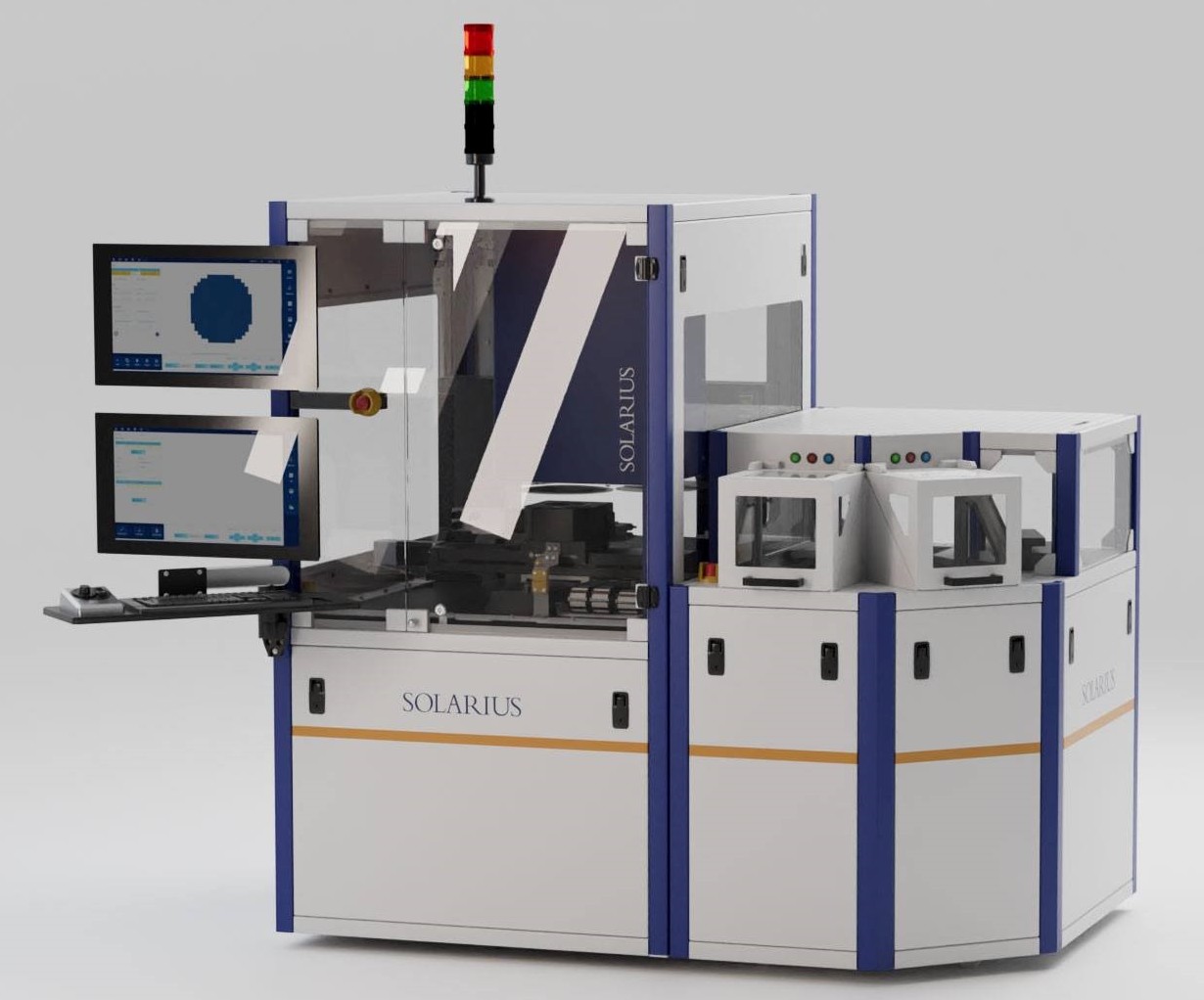
20 years of Independent 3D Machine Vision Expertise

A full line of optical 3D measurement technologies allows to choose the most cost-effective and best-in-class technical solution - regardless of manufacturer, brand or a certain technology, Solarius is your guarantee of innovation and progress in your digitized quality assurance for your Industry 4.0 approach.

The 3-dimensional detection and reproduction of technical surface properties, whether topography, texture or tribological parameters, is made possible by a variety of physically different optical imaging principles. These optical imaging principles allow a true, complete and fast digitization of technical surfaces and on this basis a real-time, automatable and reliable analysis of this data for the purpose of monitoring and controlling processes as well as for the actual assurance of the quality of products. The traceability of the quality data in the form of audit trails or subsequent verifiability of results is also possible in an easy and transparent way at any time by archiving these digitized surfaces. The optical 3D measurement technology for technical surfaces is an elementary component of the comprehensive digitization of industrial production, allowing your manufacturing lines to "visually inspect" the current process results. By its capability to make machines "see" their own action optical 3D metrology contributes to the High-Tech Project Industry 4.0

Using the various 3D imaging principles, digital images of shapes, textures, roughness and layers are created. Each of the 3D imaging principles shows natural strengths and weaknesses over the individual character of objects. Depending on the nature of a surface, the material of the workpiece, or the final use of a product, a particular imaging principle may prove advantageous over the other principles. Experience in the application of optical metrology and an independent choice of technology are essential. In addition, each of the imaging principles, over more than 20 years of intensive, industrial application of optical 3D metrology, has developed various variants of the technical implementation and design in order to best address their own natural weaknesses. The multitude of competing technologies and vendors, with all their individual advantages and disadvantages, makes choosing the right technology for a specific task or a wider range of tasks a complex and non-trivial decision.

The Solarius Group of Companies offers a broad and comprehensive portfolio of optical 3D measurement systems and technologies for digitization as well as the following metrological analysis of technical surfaces. Based on a complete technology platform, the optimal system or combination of technologies can be determined for each measurement application. Based on 20 years of experience in automated, industrial 3D measurement technology worldwide and a multinational team of experts in the field of optical 3D surface detection and image processing, Solarius is independent in choosing the most economically and technically best solution for your individual task.

Solarius SolarCore Software Platform

The Win10 Solarius SolarCore C++ software platform is designed according to industry standards, intuitively guiding engineers and operators through individual workflows. A configurable user and role management allows granular acces control. The software platform provides flexibility to a high degree as necessary to meet up-to-date requirements via its multi language C# user interface, currently availabe in English, Chinese an German. Its intelligent architecture allows quick customization, integration of new devices and is capable of processing highest amounts of data in real time processes.

The modern style user interface integrates the complete workflow of metrology and inspection tasks as well as the needed material handling capabilities by an easy and straightforward to operate functional layout. Its high level of abstraction in combination with a broad range of available metrology allows to adapt quality assurance processes to almost any objects and manufacturing environments.

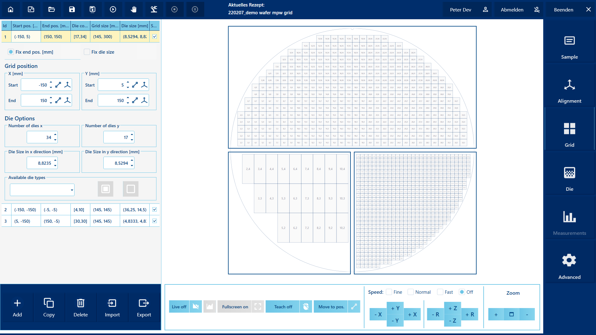
Standardized Workflow for Wafer Fabs

The SEMI wafer processing interface provides visualization and functionality for wafer handling and metrology workflows. It allows teaching of grid base recipes for wafer and panel shaped substrates, definitiontion of specification limits and the displaying of quality relevant results, taking into account the individual role rights of the current users. A detailed review of results, down to the individal items is available, same as a quick overview on cassette or FOUP/FOSB level. This user interface is the operating basis for the Solarius SIMP tools enabling diverse applications and solutions.

The semiconductor workflow allows to define data export via templating file names and folder paths, incorporating individual object data as recognized through automated QR and DDM codes within the processing of the individual wafers or panels. Material handling for fully integrated fab environments such as OHT or AGVs is availabe anlong with the SECS/GEM interface toolbox. 

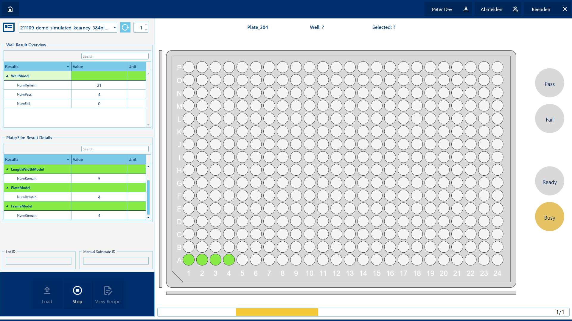
Customized Workflow for Cell Culture Plates

Besides specific user interfaces as the above semiconductor UI, a wide range of metrology and inspection tasks need highly customized user interfaces to allow operators and engineers a quick overview within their quality assurance process. With manually loaded and/or operated systems it becomes necessary to implement graphical representations of the device under test, allowing the operator a quick and clear access to result data. Also, handling related functionality has to be accessible within the same screen to avoid switching forth and back between different views throughout the operation of the tool.

The custom interface shown to the left is a special design for quality control of cell culture plates. Within this inspection and metrology task geometric and dimensional parameters of the cell culture plates have to be monitored and damages and debris have to be detected. All information becomes summarized in one consolidated view, suitable for color blind people. 

Data and Factory Interfaces

The Solarius SolarCore software platform offers different interfaces for factory automation and data transfer. The latest interface was created for the MVTec HALCON image processing library. The interface allows the generic implementation of custom image processing into the SolarCore automation environment, setting and changing input and out variabale structures for data and parameters without the need of Solarius R&D support. Besides the above, common data export interfaces for CSV or Excel as well as for customized result data structures are supported. The software platform comes along with a dual SQL server interface for process input and output data. For advanced fab automation the platform provides an OPC/UA server and client infrastructure as well as a full 300 millimeter SECS/GEM interface supporting SEMI standards E4, E5, E30, E37, E39, E40, E87, E90, E94, E116, E84 AMHS.

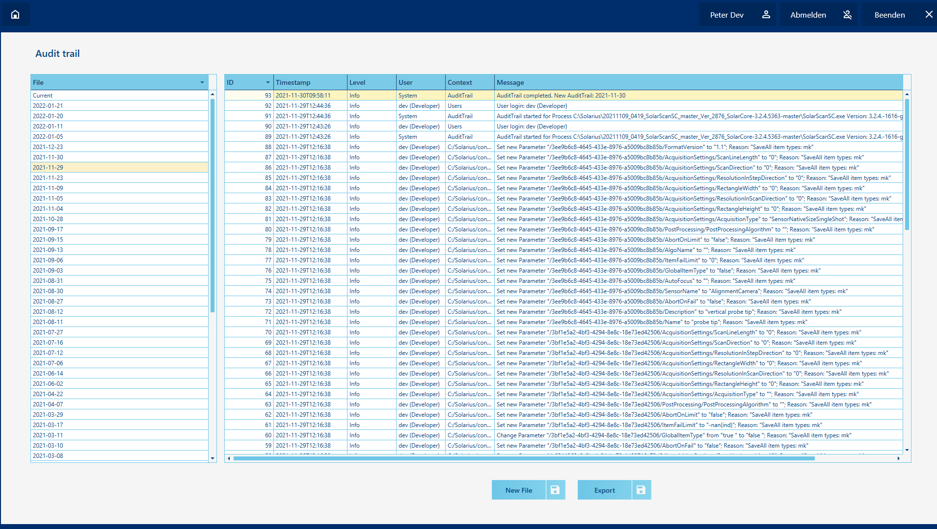
Traceability and Compliance

The integrated, FDA 21 CFR Part 11 compliant audit trail is an advanced logging data base for process relevant information as well for tracing changes and process relevant data and can be connected to electronic user identification systems as well as to the user and role management of the platform. Initially, the audit trail was designed for the SIMP tool delivered to Boehringer Ingelheim Microparts in 2020. The audit trail allows a FDA compliant and reliable tracing of all manufacturing and QA relevant changes or can be simply used as a message logging window for operator-based tool surveillance.

The software platform as well as specialized image processign algorithms follow the GAMP guidlines. The semiconductor UI workflow is implemented accordingly to the SEMI standards as applicable.

Optical Sensor Types

icons2.png

2D / 3D Optical Line Sensors

2D and 3D line sensors are ideal instruments for scanning applications where high feed rates and / or continous measurements are needed. Solarius offers various 2D and 3D chromatic or monochromatic confocal line sensor technologies as well as triangulation sensors, based on different light sources and technical implementations, applicable to a wide range of surface measurement tasks.

icons.png

2D / 3D Point Sensors

Optical point sensors are a cost efficient and space-saving alternative for various scanning metrology applications or to replace tactile profile measuring systems with up to date non contact 3D metrology. Chromatic confocal and laser point triangulation sensor technologies provide most precise and acurate results for ISO compliant measurements in the Solarius portfolio of point sensor products.

icons4.png

2D / 3D Optical Matrix Sensors

Optical matrix sensors are most common for 2D vision applications as well as for edge of technology 3D microscopy systems. The Solarius product range of matrix based sensor systems are implemented as interferometric, confocal or focus variation principles. The 3D matrix sensor systems are dedicated to edge of technology 3D measurement tasks where highest resultion and accuracy are needed.

Imaging Technologies

190419_confocal_006.png

Confocal Microscopy

Monochromatic confocal microscopy is an optical imaging technique to derive 3D surface topographies by means of using a spatial pinhole to block out-of-focus light in image formation. Capturing multiple two-dimensional images at different depths in a sample enables the reconstruction of three-dimensional structures within an object. This technique is used extensively in the scientific and industrial communities and typical applications are in life sciences, semiconductor inspection and materials science. Strength of this technology is its capability to derive very high spatial resolution and contrasts making it ideal for roughness and geometry measurements on smoth and transparent multi layer materials, rough surfaces or strongly varying reflectivities within an object. The weakness of this technology is its inability to capture steeper edges, thin layers and its comparably low measuring speed. There are high speed confocal systems available nowadays, however copared to triangulationg systems the high volume manufacturing capabilties are limited to edge of technology applications. The confocal technology can be combined with the focus variation approch to improve image quality, especially on steeper edges.

190408_chrom_confocal_006.png

Chromatic Confocal Microscopy

Chromatic confocal microscopy is related in principle to the monochromatic confocal technology. However, instead of blocking the out-of-focus light by pin holes, optical dispersion is used to create different, independent confocal conditions in different distances to the sensor. By the usage of spectroscopes or, faster and simpler by colour filters, the confocal peaks can be detected for the different wavelengths. By this colour dependent distance measurements, 3D topographies can be derived from objects and geometries. Chromatic confocal probes can measure on, and through, transparent material, detect several interfaces between materials and, therefore, calculate thickness. The metrological characteristics of point chromatic confocal systems are close to those of stylus probes and they are often used as a non-contact substitute on stylus profilometers. Strengths and weaknesses of the chromatic confocal technology are comparable to those of the monochromatic confocal approach, main differentiation is found in the comparably lower lateral resolution, a slight color sensitivity, depending on the systems technical implementation, and as a significant benefit, its comparably higher cost efficiency.

190420_interferometry_002.png

Interferometry

3D Interferometry is a measurement method using the phenomenon of interference of waves to reconstruct topographies of surfaces. In particular, displacement measuring interferometry is extensively used for the characterisation of surfaces. By using two coherent light beams, where one of it is exposed to an object's surfaces and the second one remains without modulation, an interference pattern can be formed when these two beams superpose. Because the wavelength of the visible light is very short, small changes in the differences in the optical path lengths between the two beams can be detected. Similar to confocal technology, this technique is common in life sciences, semiconductor inspection and materials science. The inherent streght of the interferometric 3D imaging technology is a very high vertical resolution, allowing to measure transparent films and layers reliaby even in the sub micron range. While interferometry still is compareably slow to triangulation systems it is a little faster than confocal approaches. Core weakness of interferometry is its limited capability in lateral resolution in respect to the confocal systems, and its high sensitivity to vibrations.

190420_holography_001.png

Holographic Interferometry

Holographic interferometry is a technique enabling static or dynamic displacements of objects with optically rough surfaces to be measured to optical interferometric precision. The measurements can be applied to stress and strain as well as to vibration analysis. Also, it can be used to detect optical path length variations in transparent media which enables, for example, fluid flow to be visualised and analyzed. Moreover, it can be used to generate contours representing the form of the surface. Holography is a process of recording diffracted light scattered from an object, then performing 3D image rendering. This process can be achieved with with a digital sensor array in digital holography. If the recorded field is superimposed on the field scattered from an ideal and plane object, the two fields will be identical. However, in case there is a small deformation on the object surface the relative phases of the light will be different and interference can be observed. Holographic interferometry can improve 3D measurement of rough surfaces while it does not overcome lateral resoultion limits and sensitivity to vibration. Its range of application for industrial 3D metrology is limited while it became a commonplace in vibrometric applications.

190420_focusvariation_004.png

Focus Variation

Focus variation based 3D sensors combine a small depth of focus of an optical system with vertical scanning to provide topography and color information from an object's surface. Using an optical system with a small depth of focus, only such parts of an object's surface are imaged in high definition which are in a certain distance to the sensor. All other areas of the surface topography appear blurred. By capturing multiple 2D images in different distances to the objects, similar to confocal systems 3D surface topographies can be reconstructed selecting the regions in high definition from each 2D image. Differentiation in an image is made, other than with pin holes in confocal systems, by the means of image processing algorithms. Focus variation is used in industrial as well as scientific applications in laboratories and mass production. Strengths of the focus variation technology certainly are, compared to confocal and interferometric approaches, its higher speed, its ability to acquire steeper edges and its capability to maintain resolution on an above triangulation level. Drawbacks are its inability to detect smooth and transparent surfaces as well as many scattering or higly dynamic 3D object topographies.

190420_triangulation_001.png

Triangulation

Triangulation sensors consits of a light pattern generating projector unit and a matrix camera imaging system. A light pattern, which can be a point, a line or even a complex arragement of color coded lines or sinusoidal patterns are projected to an object's surface. Using the example of a single line, the line will appear distorted by an uneven surface geometry or may stay a straight line when a surface is even. This distortion can be acquired by the means of the array camera. As the camera and the projector are oriented in a certain distance to each other, including a known projection and imaging angle to the object, based on the trigonometric rules of a triangle, an object's distance can be calculated. Scanning an object, a 3D topography can be derived. Triangulation is a widespread in 3D imaging with applications ranging from large automobile  parts down to geometries in the micrometer range. Triangulation provides a comparaby unmatched measurement speed, is applicable to a wide range of parts and component size and is robust against most difficult production environments. Weakness of triangulation approaches are the limited capabilty to acquire mirroring surfaces, shadowing and limitation of resolution.